Memristor is a nanoelectronic device with resistance-switching storage capabilities. It is designed to be concise, compatible with CMOS technology, and exhibits characteristics such as fast read/write operations, reasonable durability, and high-density storage capacity. These advantages make memristors a potential choice to meet future data center computing demands, demonstrating excellent performance in next-generation volatile and non-volatile memory.
Electroforming requires several volts for the formation of the conductive channel between the states before switching operations. Considering artificial synaptic sensitivity and power consumption, depletion at higher voltages is particularly crucial. Titania-based (TiO2) memristive architectures are extensively investigated, but low-forming and switching voltage architectures are rarely reported. Moreover, stability in transition metal oxide (TMO)-based memristors/ TiO2-based is not often highlighted over a period.
Recently, CenBRAIN Neurotech Center of Excellence fabricated a memristive cell bearing titania (TiOx) as the switching layer, which was deposited through atomic layer deposition (ALD). The device was characterized through X-ray photoelectron spectroscopy (XPS) and high-resolution transmission electron microscopy (HRTEM) coupled with energy-dispersive X-ray spectroscopy (XPS). The memristive cell revealed a unipolar resistive switching behavior (both at positive and negative voltages) observed through the memristor’s electrical characteristics. The observed forming/switching voltages were remarkably smaller in both directions (From top Pt electrode to grounded Au electrode, and from Au as top electrode to Pt as grounded electrode). Moreover, the retention and endurance characterization over 2000 switching cycles were satisfactory without degradation.
This contribution has been published in the IOP Nano Express Journal. Fateh Ullah, Research Assistant Professor in Westlake University, is the first author of this paper, and Mohamad Sawan, Chair Professor in Westlake University, is the corresponding author. Sincere thanks are extended to Westlake University and the Future Industries Research Center of Westlake University for their support of this work.
Reference
ULLAH F., TARKHAN M., FREDJ Z., SU Y., WANG T., SAWAN M., “A. Stable Undoped Low-voltage Memristor Cell Based on Titania (TiOx)”, IOP Nano Express Journal, Vol 5, No.1, 2023.
Abstract
An asymmetric memristive device fabricated with a titania (TiOx)-based switching layer deposited through atomic layer deposition with a thickness of ∼37 nm was investigated. X-ray photoelectron spectroscopy and high-resolution transmission electron microscopy coupled with energy-dispersive x-ray spectroscopy were employed for device structural haracterization. A unipolar resistive switching behavior (both at positive and negative voltages) was observed through the memristor’s current–voltage characteristics. A remarkably smaller forming voltage (from the top Pt electrode to the grounded Au electrode) of 0.46 V was achieved, while it approached (positive bias from the Au electrode and holding Pt electrode as grounded) 0.25 V, which is a much smaller forming voltage than has ever been reported for titanium-based oxides without doping. The retention and endurance characterization over 2000 switching cycles were satisfactory without degradation.
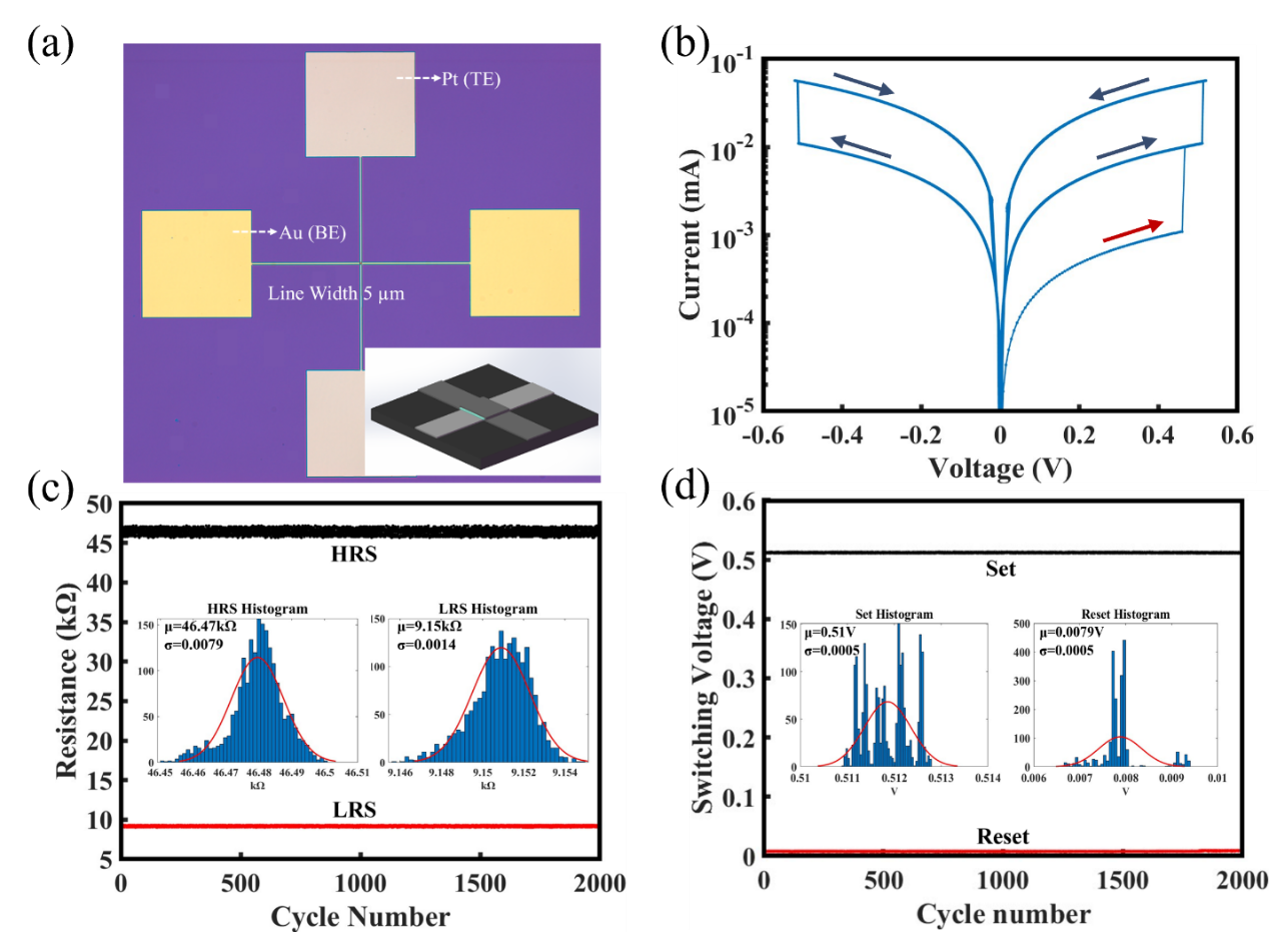
Fig. 1: (a) Optical image of the crossbar structure of Pt/Cr/TiOx/Au/SiO2/Si device, (b) Plot of the I-V curve of the device recorded for 2000-voltage sweeps, (c) HRS and LRS state values, and (d) Set and Reset voltages recorded.
To the best of our knowledge, it’s the first example of such a low-forming voltage than the switching voltage for TiOx-based memristive cells. Besides, it’s the lowest reported forming and switching voltage for TiOx-based non-diffusive memristive architectures. Moreover, the first example that follows Ohm’s law both at HRS and LRS.
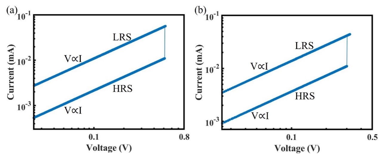
Fig. 2: Log–log plot of the I–V characteristics in the positive voltage region displaying unity slope at both HRS and LRS switching: (a) at 0.51 V (voltage given from Pt electrode while Au was grounded), and (b) at 0.3 V (voltage given from Au electrode while Pt was grounded).
More information can be found at the following link:
https://iopscience.iop.org/article/10.1088/2632-959X/ad1413


